Tamper Detection Meshes
Cryptography is at the foundation of our modern, networked world. From email to card payment infrastructure in brick and
mortar stores, cryptographic keys secure almost every part of our digital lives againts cybercriminals or curious
surveillance capitalists. Without cryptography, many of the things we routinely do in our lives such as paying for
groceries with a credit card, messaging a friend on Signal or unlocking a car with its keyfob
would not be possible. The security of all of these systems in its core lies on the secrecy of cryptographic keys.
Systems differ in what kind of keys they use, how often these keys are replaced and the intricacies of the cryptographic
operations these keys fit into but all have in common that their security relies on keeping the keys secret.
In practice, this secrecy has been implemented in many different ways. Mass-market software such as browsers or
messenger apps usually relies on some operating system facility to tell the computer "please keep this piece of memory
away from all other applications". While on desktop operating systems usually this does not provide much of a barrier
to other programs on the same computer, on modern mobile operating systems this approach is actually quite secure.
However, given sufficient resources no security is perfect. All of these systems can be compromised if the host
operating system is compromised sufficiently, and for organizations with considerable resources a market has sprung up
that offers turn-key solutions for all wiretapping needs.
In some applications, this level of security has not been considered sufficient. Particularly financial infrastructure
is such a high-profile target that a lot of effort has been put into the security of cryptographic implementations. The
best cryptographic algorithm is useless if it is run on a compromised system (from that system's point of view anyway).
One of the core cryptographic components in financial applications are smartcards like they are used as payment cards in
most countries nowadays. These smartcards contain a small, specialized cryptographic microcontroller that is designed to
be hard to tamper with. Though one of the design goals of the system is to reduce the amount of sensitive information
stored on the card, things such as copying of a card can only be hindered by making the chip hard to read out.

With smartcards being the means of choice on one side of the counter in electronic payments, on the other side of the
counter a different technology prevails. Attacks on payment terminals are bound to have much more dire consequences than
attacks on individual cards since one terminal might see hundreds of cards being read every day. For this reason, the
level of attack countermeasures employed in these terminals is a considerable step up from bare smartcards. While a
smartcard is made physically hard to tamper, it does not have a battery and it can only detect tampering once it is
powered by a reader. This allows for well-equipped attackers to use tools such as Focused Ion Beam (FIB) workstations to
circumvent the smartcard's defences while it is powered down, and then power up the card to carry out the actual attack.
The answer to this problem in electronic payment infrastructure is called Hardware Security Module, or HSM. An HSM is
similar to a smartcard in its function (cryptographic processing using keys that are meant to never leave the protection
of the HSM). The one major between the two is that an HSM has its own battery and is continuously powered from its
manufacture to the day it is scrapped. If the HSM looses power at any point in time, it uses a small amount of energy
stored internally to securely wipe all cryptographic secrets from its memory within a few milliseconds.
Being powered at all times allows the HSM to actively detect and respond to attacks. The most common way this is done is
by wrapping the juicy secret parts in a foil or a printed circuit board that is patterned with a long and convoluted
maze of wires, called a mesh. The HSM is continuously monitoring these wires for changes (such as shorts, breaks or
changes in resistance) and will sound the alarm when any are detected. Practically, this presents a considerable hurdle
to any attacker: They have to find a way to disable or circumvent the mesh while it is being monitored by the HSM. In
practice, often this is no insurmountable challenge but it again increases attack costs.
DIY Meshes
Throughout my studies in security research I have always had an interest in HSMs. I have taken apart my fair share of
HSMs and at this point, to understand the technology more, I want to experiment with building my own HSM. In last year's
HSM basics post I have lined out some ideas for a next generation design that
deviates from the bread-and-butter apporoach of using a mesh as the primary security feature. Before embarking on
practical experiments with these ideas, I want to first take a stab at replicating the current state of the art as best
I can. State of the art meshes often use exotic substrates such as 3D plastic parts with traces chemically deposited on
their surface or special flexible substrates with conductive ink traces. These technologies will likely be too
cumbersome for me to implement myself only for a few prototypes, and industrial manufacturers will most likely be too
expensive. Thus, I will concentrate on regular PCB technology for now.
The idea of a mesh on a PCB is pretty simple: You have one or several traces that you try to cover every corner of the
mesh PCB's area with. To be most effective, the traces should be as thin and as close together as possible. To increase
the chances of a manipulation being detected, multiple traces can also be used that can then be monitored for shorts
between them.
While one can feasibly lay out these traces by hand, this really is an ideal application of a simple auto-router. While
general PCB autorouting is hard, auto-routing just a few traces to approximate a space-filling curve is not. Since I
am just starting out, I went with the simplest algorithmic solution I could think of. I first approximate the area
designated to the mesh with a square grid whose cells are a multiple of my trace/space size. The mesh will only be drawn
into grid cells that are fully inside the set boundaries. All cells outside or going across the border are discarded in
this step.
I decided to implement this auto-router in a KiCAD plugin. Though KiCADs plugin API is not the best, it was just about
usable for this task.
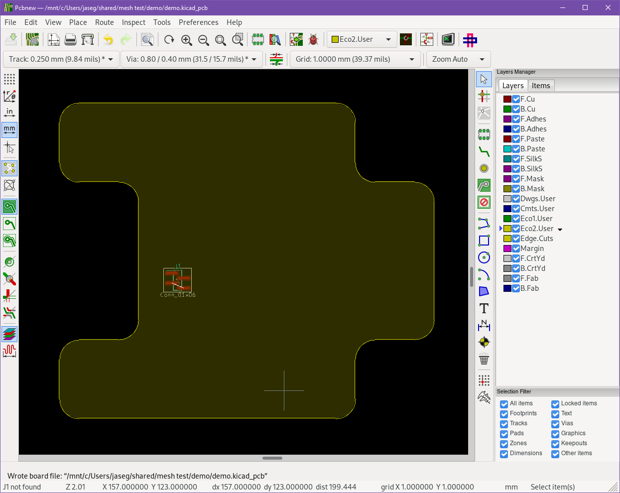 The process starts out with the mesh shape being defined inside KiCAD. The mesh's outline is drawn
onto one of the graphical "Eco" layers. A footprint is placed to serve as a placeholder for the mesh's
connections to the outside world. This footprint is later used as the starting point for the mesh generation
algorithm.
The process starts out with the mesh shape being defined inside KiCAD. The mesh's outline is drawn
onto one of the graphical "Eco" layers. A footprint is placed to serve as a placeholder for the mesh's
connections to the outside world. This footprint is later used as the starting point for the mesh generation
algorithm.
 A visualization of the grid fitting process. First, a grid large enough to contain the mesh border
is generated. Then, every cell is checked for overlap with the mesh border area. If the cell is fully inside, it
(yellow), it is considered in the mesh generation later. Cells outside (gray) or on the border (red) are
discarded.
A visualization of the grid fitting process. First, a grid large enough to contain the mesh border
is generated. Then, every cell is checked for overlap with the mesh border area. If the cell is fully inside, it
(yellow), it is considered in the mesh generation later. Cells outside (gray) or on the border (red) are
discarded.
After generating the grid, starting from the place I want to connect to the mesh, I walk the grid's cells one by one to
generate a tree that covers the entire grid's area. To set the mesh's starting place I place a footprint on the board
(dark gray in the picture above) whose designator I then tell my script. The tree generation algorithm looks like a
depth-first search, except all checks are random. Depending on the level of randomness used at each step of the
algorithm it yields more or less organized-looking results. Below are five example runs of the algorithm at differing
levels of randomness with the cells colored according to their distance from the tree root. 0% randomness means that the
algorithm is going to try cells in forward direction first on every step, and only then try out left and right. 100%
means that on every step, the algorithm is choosing a new direction at random.
After I have built this tree like you would do in a depth-first search, I draw my one or several mesh mesh traces into
it. The core observation here is that there is only 16 possible ways a cell can be connected: It has four neighbors,
each of which it can either be connected to or not, which results in 2^4 options. If you consider rotations and
mirroring, this works out to rotations or mirrored versions of only six base tiles: The empty tile, a tile with all four
sides connected, a straight through, a 90 degree bend, and a "T"-junction—see the illustration below.
 There are six possible tile types in our connectivity graph inside its square tiling. This graphic illustrates
all sixteen rotations of these with how they would look in a two-conductor mesh.
There are six possible tile types in our connectivity graph inside its square tiling. This graphic illustrates
all sixteen rotations of these with how they would look in a two-conductor mesh.
After tiling the grid according to the key above, we get the result below.
 An auto-routed mesh with traces colored according to tile types.
 The same mesh, but with traces all black.
Putting it all together got me the KiCAD plugin you can see in the screenshot below.
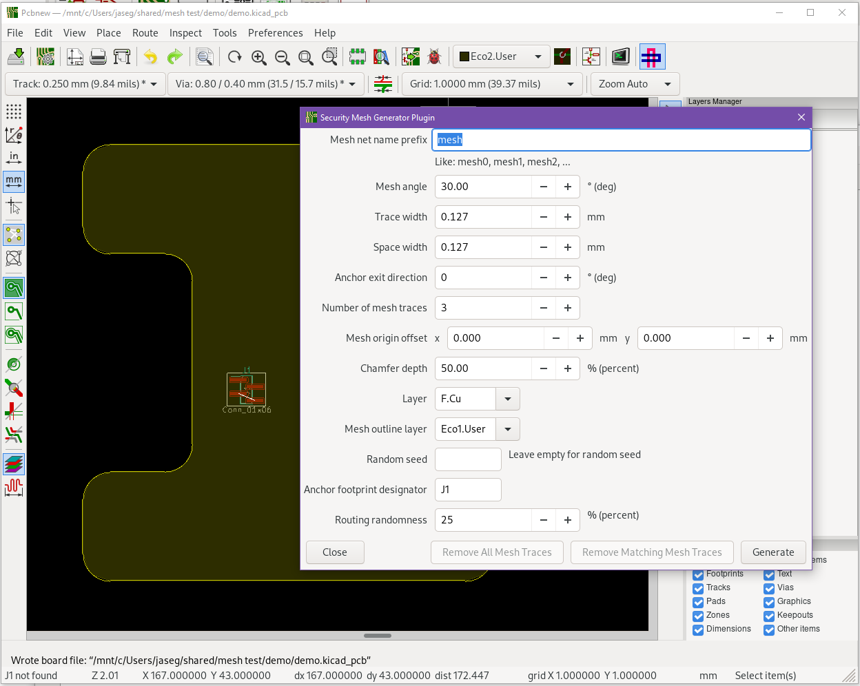 The plugin settings window open.
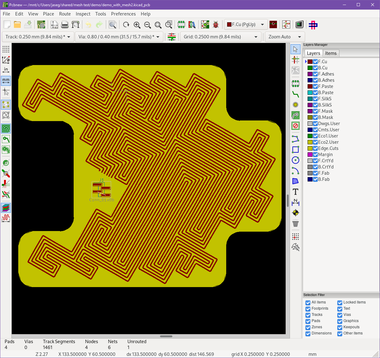 After runing the plugin, the generated mesh looks like this in pcbnew.
I am fairly happy with the result, but getting there was a medium pain. Especially KiCAD's plugin API is still very
unfinieshed. It is hard to use, most parts are completely undocumented and if you use anything but its most basic parts
things tend to break. One particular pain point for me was that after generating the mesh, the traces have been added to
the board, but are still invisible for some reason. You have to save the board first, then re-load the file for them to
become visible. Also KiCAD crashes whenever the plugin tries to remove a trace, so currently my workflow involves always
making a copy of the board file first and treating mesh generation as a non-reversible finishing step.
Check out the code on my cgit.